- 您现在的位置:买卖IC网 > Sheet目录3861 > PIC18F45K80-I/ML (Microchip Technology)MCU PIC 32KB FLASH 44QFN
2010-2012 Microchip Technology Inc.
DS39977F-page 171
PIC18F66K80 FAMILY
11.0
I/O PORTS
Depending on the device selected and features
enabled, there are up to seven ports available. Some
pins of the I/O ports are multiplexed with an alternate
function from the peripheral features on the device. In
general, when a peripheral is enabled, that pin may not
be used as a general purpose I/O pin.
Each port has three memory mapped registers for its
operation:
TRIS register (Data Direction register)
PORT register (reads the levels on the pins of the
device)
LAT register (Output Latch register)
Reading the PORT register reads the current status of
the pins, whereas writing to the PORT register, writes
to the Output Latch (LAT) register.
Setting a TRIS bit (= 1) makes the corresponding port
pin an input (putting the corresponding output driver in
a High-Impedance mode). Clearing a TRIS bit (= 0)
makes the corresponding port pin an output (i.e., put
the contents of the corresponding LAT bit on the
selected pin).
The Output Latch (LAT register) is useful for
read-modify-write operations on the value that the I/O
pins are driving. Read-modify-write operations on the
LAT register read and write the latched output value for
the PORT register.
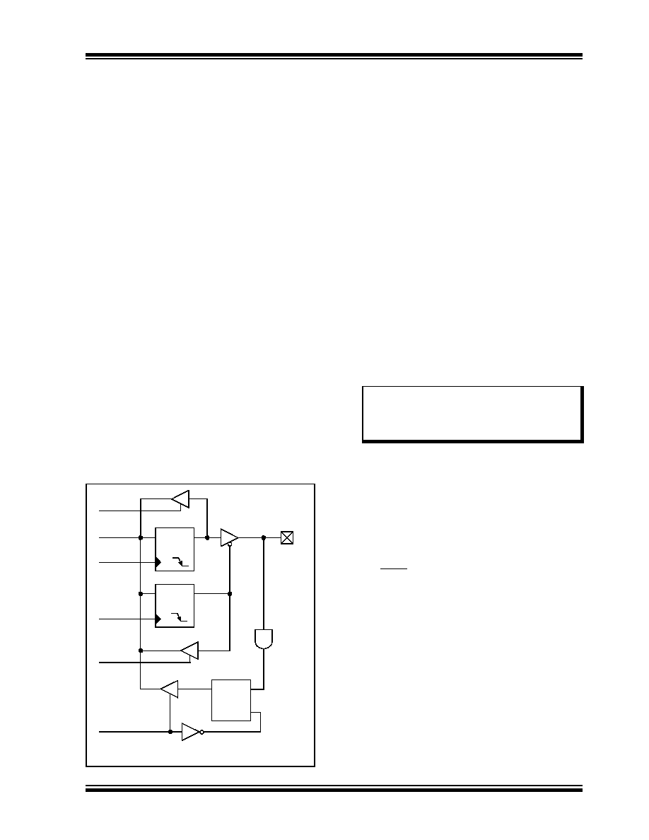
A simplified model of a generic I/O port, without the
interfaces to other peripherals, is shown in Figure 11-1.
FIGURE 11-1:
GENERIC I/O PORT
OPERATION
11.1
I/O Port Pin Capabilities
When developing an application, the capabilities of the
port pins must be considered. Outputs on some pins
have higher output drive strength than others. Similarly,
some pins can tolerate higher than VDD input levels.
All of the digital ports are 5.5V input tolerant. The
analog ports have the same tolerance, having clamping
diodes implemented internally.
11.1.1
PIN OUTPUT DRIVE
When used as digital I/O, the output pin drive strengths
vary, according to the pins’ grouping to meet the needs
for a variety of applications. In general, there are two
classes of output pins, in terms of drive capability:
Outputs that are designed to drive higher current
loads, such as LEDs:
-PORTA
– PORTB
-PORTC
Outputs with lower drive levels, but capable of
driving normal digital circuit loads with a high input
impedance. Able to drive LEDs, but only those
with smaller current requirements:
-PORTD(1)
–PORTE(1)
-PORTF(2)
–PORTG(2)
For more details, see “Absolute Maximum Ratings” in
11.1.2
PULL-UP CONFIGURATION
Five of the I/O ports (PORTB, PORTD, PORTE,
PORTF and PORTG) implement configurable weak
pull-ups on all pins. These are internal pull-ups that
allow floating digital input signals to be pulled to a
consistent level without the use of external resistors.
The pull-ups are enabled with a single bit for each of the
ports: RBPU (INTCON2<7>) for PORTB, and RDPU,
REPU, RFPU and RGPU (PADCFG1<7:4>) for the
other ports.
Additionally, the PORTB pull-up resistors can be
enabled individually using the WPUB register. Each bit
in the register corresponds to a bit on PORTB.
Data
Bus
WR LAT
WR TRIS
RD PORT
Data Latch
TRIS Latch
RD TRIS
Input
Buffer
I/O Pin(1)
Q
D
CKx
Q
D
CKx
EN
QD
EN
RD LAT
or PORT
Note 1:
I/O pins have diode protection to VDD and VSS.
Note 1:
These ports are not available on 28-pin
devices.
2:
These ports are not available on 28-pin
or 40/44-pin devices
发布紧急采购,3分钟左右您将得到回复。
相关PDF资料
PIC24F32KA302-I/ML
MCU 32KB FLASH 2KB RAM 28-QFN
PIC18LF45K80-I/ML
MCU PIC ECAN 32KBFLASH 44QFN
PIC18F4221-I/PT
IC PIC MCU FLASH 2KX16 44TQFP
PIC18F1320-I/SO
IC MCU FLASH 4KX16 A/D 18SOIC
PIC18LF2321-I/SS
IC PIC MCU FLASH 4KX16 28SSOP
PIC16F917-I/PT
IC PIC MCU FLASH 8KX14 44TQFP
PIC18F1320-I/SS
IC MCU FLASH 4KX16 A/D 20SSOP
PIC24FV32KA301-I/P
MCU 32KB FLASH 2KB RAM 20-PDIP
相关代理商/技术参数
PIC18F45K80-I/P
功能描述:8位微控制器 -MCU 32KB FL 4KBRM 16MIPS 12bit ADC CTMU RoHS:否 制造商:Silicon Labs 核心:8051 处理器系列:C8051F39x 数据总线宽度:8 bit 最大时钟频率:50 MHz 程序存储器大小:16 KB 数据 RAM 大小:1 KB 片上 ADC:Yes 工作电源电压:1.8 V to 3.6 V 工作温度范围:- 40 C to + 105 C 封装 / 箱体:QFN-20 安装风格:SMD/SMT
PIC18F45K80-I/PT
功能描述:8位微控制器 -MCU 32KB FL 4KBRM 16MIPS 12bit ADC CTMU RoHS:否 制造商:Silicon Labs 核心:8051 处理器系列:C8051F39x 数据总线宽度:8 bit 最大时钟频率:50 MHz 程序存储器大小:16 KB 数据 RAM 大小:1 KB 片上 ADC:Yes 工作电源电压:1.8 V to 3.6 V 工作温度范围:- 40 C to + 105 C 封装 / 箱体:QFN-20 安装风格:SMD/SMT
PIC18F45K80T-I/ML
功能描述:8位微控制器 -MCU 32KB FL 4KBRM 16MIPS 12bit ADC CTMU RoHS:否 制造商:Silicon Labs 核心:8051 处理器系列:C8051F39x 数据总线宽度:8 bit 最大时钟频率:50 MHz 程序存储器大小:16 KB 数据 RAM 大小:1 KB 片上 ADC:Yes 工作电源电压:1.8 V to 3.6 V 工作温度范围:- 40 C to + 105 C 封装 / 箱体:QFN-20 安装风格:SMD/SMT
PIC18F45K80T-I/PT
功能描述:8位微控制器 -MCU 32KB FL 4KBRM 16MIPS 12bit ADC CTMU RoHS:否 制造商:Silicon Labs 核心:8051 处理器系列:C8051F39x 数据总线宽度:8 bit 最大时钟频率:50 MHz 程序存储器大小:16 KB 数据 RAM 大小:1 KB 片上 ADC:Yes 工作电源电压:1.8 V to 3.6 V 工作温度范围:- 40 C to + 105 C 封装 / 箱体:QFN-20 安装风格:SMD/SMT
PIC18F4610-E/ML
功能描述:8位微控制器 -MCU 64KB 3968 RAM 36 I/O RoHS:否 制造商:Silicon Labs 核心:8051 处理器系列:C8051F39x 数据总线宽度:8 bit 最大时钟频率:50 MHz 程序存储器大小:16 KB 数据 RAM 大小:1 KB 片上 ADC:Yes 工作电源电压:1.8 V to 3.6 V 工作温度范围:- 40 C to + 105 C 封装 / 箱体:QFN-20 安装风格:SMD/SMT
PIC18F4610-E/P
功能描述:8位微控制器 -MCU 64KB 3968 RAM 36 I/O RoHS:否 制造商:Silicon Labs 核心:8051 处理器系列:C8051F39x 数据总线宽度:8 bit 最大时钟频率:50 MHz 程序存储器大小:16 KB 数据 RAM 大小:1 KB 片上 ADC:Yes 工作电源电压:1.8 V to 3.6 V 工作温度范围:- 40 C to + 105 C 封装 / 箱体:QFN-20 安装风格:SMD/SMT
PIC18F4610-E/PT
功能描述:8位微控制器 -MCU 64KB 3968 RAM 36 I/O RoHS:否 制造商:Silicon Labs 核心:8051 处理器系列:C8051F39x 数据总线宽度:8 bit 最大时钟频率:50 MHz 程序存储器大小:16 KB 数据 RAM 大小:1 KB 片上 ADC:Yes 工作电源电压:1.8 V to 3.6 V 工作温度范围:- 40 C to + 105 C 封装 / 箱体:QFN-20 安装风格:SMD/SMT
PIC18F4610-I/ML
功能描述:8位微控制器 -MCU 64KB 3968 RAM 36 I/O RoHS:否 制造商:Silicon Labs 核心:8051 处理器系列:C8051F39x 数据总线宽度:8 bit 最大时钟频率:50 MHz 程序存储器大小:16 KB 数据 RAM 大小:1 KB 片上 ADC:Yes 工作电源电压:1.8 V to 3.6 V 工作温度范围:- 40 C to + 105 C 封装 / 箱体:QFN-20 安装风格:SMD/SMT